
How to Reduce Inrush Current in MOSFET Power Switches
1 Introduction
On a real-world project, we used a P-channel MOSFET as a high-side switch to control the power supply of a sensor. The basic circuit is shown in Figure 1.
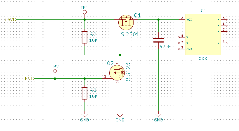
Figure 1 – Original P-channel MOSFET high-side switch used to control the sensor supply
At first glance, the task was simple: use a control signal to turn the sensor’s power supply on or off.
However, the sensor drew a relatively high current during startup. In addition, an external capacitor was connected to its VDD supply. At the moment of turn-on, this capacitor behaves as an additional load and requires charging current. As a result, turning on the sensor produced a significant inrush current, accompanied by a voltage drop on the supply rail.
The device worked without any problems with the originally selected P-MOSFET. However, during production, that particular transistor was no longer available, so we selected a replacement MOSFET from another manufacturer. According to the datasheets, both transistors had practically identical characteristics, including the specification RDS(on) < 10 Ω.
Nevertheless, the replacement transistor did not work in our circuit.
At first, this seemed rather unusual. If both MOSFETs met the same RDS(on) requirement, why would one work while the other did not?
The answer turned out to be more interesting than expected. The original transistor had a higher actual RDS(on) in the circuit, while the replacement transistor had a lower RDS(on). A difference that would normally be considered an advantage in a MOSFET was precisely what caused the problem in this particular application.
The MOSFET with the lower RDS(on) allowed a higher current to flow during turn-on. The capacitor on the sensor’s VDD supply charged more quickly, the current surge was higher, and the result was a larger instantaneous voltage drop on the supply rail. Because of this, the sensor did not start up correctly.
Furthermore, the specification RDS(on) < 10 Ω in a datasheet does not mean that two transistors have the same resistance. It is only a guaranteed upper limit under specified measurement conditions. The actual RDS(on) of an individual transistor can be significantly different, even when both devices satisfy the same datasheet specification.
This led to an interesting conclusion: the problem was not that the replacement MOSFET was “worse.” On the contrary, it was better in terms of RDS(on), but precisely because of that, it allowed too much current to flow during turn-on.
The solution was therefore not to search for a MOSFET with the “right” RDS(on) value, but to control how the MOSFET is turned on.
Instead of switching the P-MOSFET directly from OFF to ON, we can control its turn-on rate. This allows us to limit the current used to charge the capacitor on the sensor’s VDD supply and reduce the resulting voltage drop.
2 The Problem: Voltage Drop During Turn-On
To better understand what was happening during startup, we captured the sensor supply voltage with an oscilloscope. The resulting waveform is shown in Figure 2.
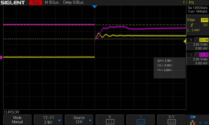
Figure 2 – Measured sensor supply voltage during turn-on with the replacement MOSFET
Oscilloscope measurement clearly shows what happens during sensor startup. Immediately after the supply is switched on, a significant voltage drop occurs on the sensor’s VDD rail. According to the cursor measurement, the difference between the marked voltage levels is approximately 2.16 V. The supply voltage then recovers and settles to its normal operating level.
This measurement confirms that the problem occurs during the turn-on transient rather than during steady-state operation. Once the transient has passed, the supply reaches a stable voltage, but the initial voltage drop is large enough to prevent the sensor from starting correctly.
2.1 Lower RDS(on) Is Not Always Better
For a MOSFET used as a switch, a lower RDS(on) is generally desirable. It means a lower voltage drop across the device and lower conduction losses during normal operation.
However, RDS(on) tells us very little about what happens during the turn-on transient.
In our case, the steady-state current was not a problem. Once the sensor was powered, the voltage drop across the MOSFET and its conduction losses were within acceptable limits. The critical moment was the transition from the OFF state to normal operation.
During this short interval, the MOSFET had to provide both the current required to start the sensor and the current required to charge the external capacitor on the VDD supply. Therefore, what mattered was no longer simply how much voltage the MOSFET dropped when fully turned on, but how much current the circuit would allow to flow during turn-on and how quickly the sensor supply voltage would rise.
This highlights an important distinction between steady-state behavior and transient behavior. We can have a MOSFET with very good RDS(on) characteristics while still having no control over its behavior during turn-on.
Therefore, instead of relying on the MOSFET’s RDS(on) as an accidental current limiter, we need to control the rate at which the MOSFET turns on.
3 Controlling the MOSFET Turn-On
The previous measurements showed that the critical part of the sensor startup occurs during the turn-on transient. Instead of relying on the MOSFET’s RDS(on) as an accidental current limiter, we can control the way the MOSFET is turned on. The basic idea is to slow down the rise of the sensor supply voltage. If the voltage across the external VDD capacitor is allowed to increase gradually, the current required to charge it can be reduced:Therefore, by controlling the MOSFET’s turn-on rate, we can influence the current flowing during sensor startup. The goal is not to slow the MOSFET down during normal operation, but to control only the turn-on transient.
For this purpose, we looked at the load-switch topology shown in Figure 3, taken from Figure 16 of the Onsemi FDC6324L datasheet.
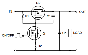
Figure 3 – Load-switch topology from the Onsemi FDC6324L datasheet
The topology uses two MOSFETs. Q2 is a P-channel MOSFET used as the high-side switch, while Q1 is an N-channel MOSFET that controls the gate of Q2. When Q1 is turned on, it pulls the gate of Q2 toward ground, causing Q2 to turn on and connect the input supply to the load.
R1 provides the pull-up path for the gate of Q2. When Q1 is off, the gate of Q2 is pulled toward the input voltage, keeping the P-channel MOSFET turned off.
A particularly important component in this topology is R2, which is placed in the source of Q1. When Q1 conducts, the current flowing through R2 creates a voltage drop across it. This limits the current through Q1 and therefore controls how quickly the gate of Q2 is discharged. As a result, the turn-on of the P-channel MOSFET can be made slower and more controlled.
The topology also includes C1, which provides additional control of the turn-on behavior. By introducing additional capacitance around the gate of Q2, the turn-on transition can be slowed further when required.
For our first experiment, however, we did not use C1. We adapted the basic topology to our 3.3 V application using the NDS352AP as Q2, the P-channel high-side MOSFET, and the BSS123 as Q1, the N-channel control MOSFET. We initially focused on the effect of R2 alone and how it changes the turn-on transient of the high-side switch.
4 The Solution: Reducing the Voltage Drop
After analyzing the controlled turn-on principle in the previous section and adapting the topology to our circuit, the next step was to verify how this modification would behave in the actual device.
In the first version of the experiment, we added R2 to the source of the BSS123, without the additional C1 capacitor. The goal was to limit the current through the BSS123 and thereby control the rate at which the P-MOSFET gate was pulled toward ground.
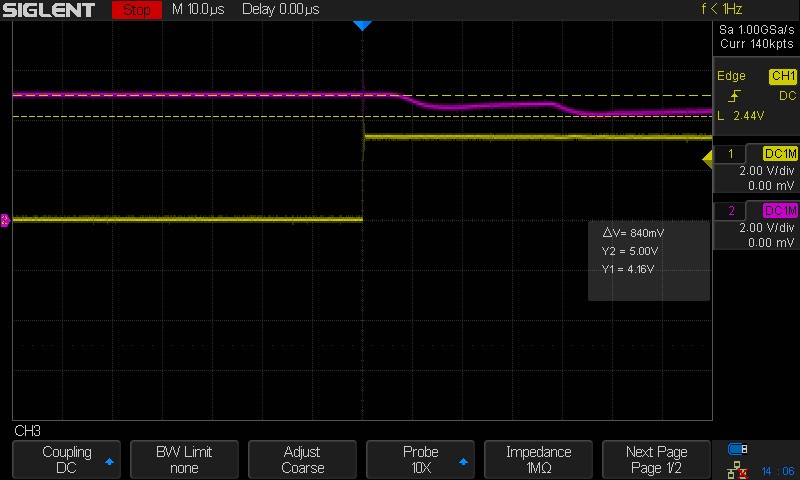
Figure 4 – Oscilloscope measurement of the sensor supply during turn-on with the added R2 resistor
The waveform shows that the voltage drop during turn-on is now significantly smaller. In the previous measurement, shown in Figure 2, the measured voltage drop was approximately 2.16 V, while after adding R2, it was reduced to approximately 840 mV.
This represents a reduction of approximately 61% in the measured voltage drop.
More importantly, this modification solved the sensor startup problem. We did not change the P-MOSFET or try to select a transistor based on a particular RDS(on) value. Instead, we changed the way the high-side switch was controlled, thereby reducing the current surge during startup.
This experiment showed that the problem could not be attributed solely to the MOSFET or its RDS(on). The startup behavior was influenced by a combination of the sensor’s startup requirements, the external VDD capacitor, the inrush current, and the characteristics of the high-side switch. By controlling the turn-on transient, we were able to significantly reduce the voltage drop and achieve reliable sensor startup.
5 The Final Circuit
Based on the results of this experiment, we defined the final version of the circuit. Figure 5 shows our modified 3.3 V high-side switch, based on the topology presented in Figure 3 and adapted to the specific components used in our project.
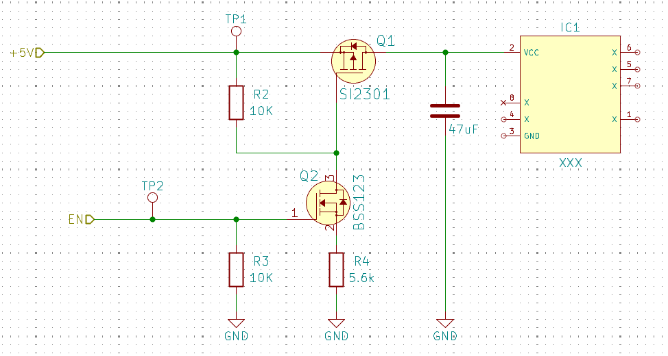
Figure 5 – Final version of the 3.3 V high-side switch using the NDS352AP and BSS123
In our case, R2 was 5.6 kΩ. This value was determined experimentally for the specific combination of the NDS352AP and BSS123. It is important to note that this value should not be considered universal for all MOSFETs. Increasing R2 limits the current through the BSS123 and further slows down the turn-on of the P-MOSFET, but an excessively large value can result in insufficient VGS to turn the P-MOSFET on reliably.
As a starting guideline, a ratio of approximately 10:1 between the resistor connected between the source and gate of the P-MOSFET and R2 can be considered, but this ratio is not a strict rule. In our experiment, we also tested values outside this ratio and found that 5.6 kΩ provided the desired behavior in our particular circuit while still allowing the NDS352AP to turn on reliably.
The final value of R2 is therefore a trade-off between turn-on speed and sufficient gate drive, and should be verified for the specific combination of MOSFET, supply voltage, and required turn-on time.

Amar Degirmendžić
Senior Embedded Hardware Engineer
Amar Degirmendžić (E76DA) is an Senior Embedded Hardware Engineer and amateur radio operator interested in electronic system design, RF systems, and measurement techniques. His work ranges from schematic capture and PCB design to hands-on circuit assembly, testing, and practical laboratory measurements

S