
Simulation vs. Reality
Evaluating the Accuracy of MOSFET Switching Models1 Introduction
Circuit simulation has become an indispensable tool in modern electronic design. It allows engineers to evaluate different design ideas, verify circuit functionality, and analyze circuit behavior before building the first hardware prototype. As a result, development time is reduced, design iterations become faster, and overall costs are significantly lower.
Of course, every simulation is only a mathematical representation of a real circuit. The accuracy of the results largely depends on the quality of the component models and on how many real-world effects are included in the simulation, such as parasitic resistance, capacitance, and inductance. On the other hand, real-world measurements are not perfect either. Measurement equipment, oscilloscope probes, PCB traces, wires, and even the physical layout introduce additional parasitic elements that influence the observed waveforms.
For this reason, the goal of this article is not to prove whether circuit simulation is “right” or “wrong,” nor to claim that laboratory measurements represent an absolute reference. In practice, simulation and measurement complement each other. Simulation helps us understand circuit behavior before hardware is built, while measurements confirm how the same circuit performs under real operating conditions.
Like many beginners, we often wondered how closely SPICE simulation results resemble what we eventually observe on an oscilloscope. Are the differences negligible, or can they become significant? How much of the discrepancy comes from simplified device models, and how much is caused by the unavoidable parasitic elements of a real circuit?
In this article, we will explore these questions by comparing LTspice simulation results with real oscilloscope measurements using a simple MOSFET switching circuit. Both the simulation and the experimental setup will use the same operating conditions and measurement methodology. The objective is not to determine a “winner,” but rather to identify where simulation and reality agree, where they differ, and to discuss the most common reasons behind those differences.
2 Experimental Setup
To ensure a fair and objective comparison between LTspice simulation results and real-world measurements, a simple MOSFET switching circuit was built and tested under controlled laboratory conditions. The same circuit topology, component values, and operating conditions were used in both the simulation and the physical experiment.
An IRFZ44N N-channel power MOSFET was used as the switching device in a low-side switch configuration. The MOSFET gate was driven by a square-wave signal generated by a function generator, while a 10 kΩ pull-down resistor ensured that the transistor remained in the OFF state whenever no gate drive signal was present. A series gate resistor was placed between the function generator and the MOSFET gate to control the gate charging and discharging current. Two gate resistor values were investigated during the experiments: 10 Ω and 100 Ω.
A 94 Ω purely resistive load powered from a 12 V DC supply was selected as the load. A resistive load was intentionally chosen to eliminate the influence of inductive energy storage and other complex transient effects, allowing for a more straightforward comparison between simulation and experimental results. The behavior of the MOSFET under inductive and other load types will be investigated in future articles.
Measurements were performed using a Siglent SDS2304X digital oscilloscope, while the gate drive signal was generated by a Siglent SDG1062X function/arbitrary waveform generator. The generator was configured to produce a 0–5 V square wave at a frequency of 20 kHz with a 50% duty cycle. The generator output rise and fall times were measured to be approximately 4 ns, and the same values were used to define the input signal in the LTspice simulation.
The complete circuit used throughout this study is shown in Figure 1.
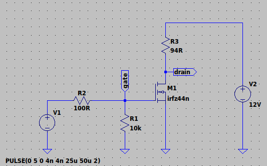
Figure 1 – LTSpice schematic of the experimental MOSFET switching circuit
Before comparing the simulation and experimental results, it is important to define which electrical quantities will be evaluated and how they will be measured. Throughout this article, the comparison will focus on the rise time and fall time of both the gate and drain voltages. To ensure consistency, the same measurement methodology—using the 10% to 90% transition levels—will be applied in both LTspice and the oscilloscope measurements.
3 Measurement Methodology
To ensure an objective comparison between LTspice simulations and real-world laboratory measurements, the same circuit schematic, the same IRFZ44N MOSFET, and identical operating conditions were used throughout the study. The objective was to ensure that the only difference between the results originated from the method of analysis itself—simulation versus experimental measurement.
The simulation results were obtained using LTspice, while the experimental measurements were performed with a Siglent SDS2304X digital oscilloscope. In both cases, the same electrical quantities were observed: the gate voltage and the drain voltage.
This article focuses on comparing the rise time and fall time of these signals. These parameters are among the most commonly used indicators of a transistor’s switching performance and provide a straightforward way to evaluate the agreement between simulation and experimental results.
According to standard engineering practice, rise time is defined as the time required for a signal to transition from 10% to 90% of its final amplitude, while fall time is defined as the time required for a signal to transition from 90% to 10% of its amplitude. The same measurement methodology was applied in both the LTspice simulation and the oscilloscope measurements, allowing for a direct and meaningful comparison of the obtained results.
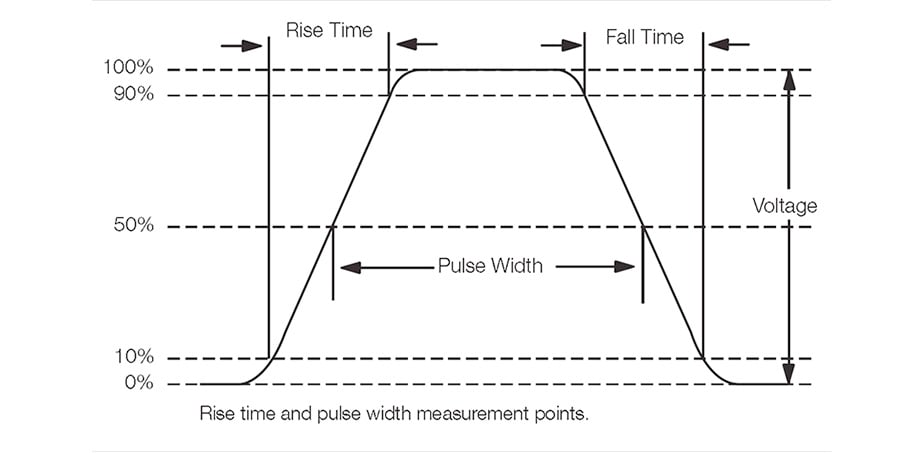
Figure 2 – Standard 10%-90% definition of rise time and fall time
4 LTSpice Simulation
Before assembling the experimental circuit, the switching behavior of the MOSFET was analyzed using LTspice. The simulation was performed under the same operating conditions as the laboratory experiment, using identical component values and the manufacturer-provided SPICE model of the IRFZ44N MOSFET.
A transient analysis was carried out to observe the switching waveforms at the gate and drain terminals. The same gate drive signal used in the laboratory measurements—a 0–5 V square wave at 20 kHz—was applied in the simulation. To ensure a fair comparison, the measured 4 ns rise and fall times of the function generator output were also incorporated into the simulation.
The rise time and fall time of both the gate and drain voltages were determined using LTspice measurement directives, following the 10%–90% measurement criterion described in the previous section. The obtained waveforms and measurement results are presented below.
In all LT spice screenshots presented in this article, the green trace corresponds to the gate voltage, whereas the red trace corresponds to the drain voltage.
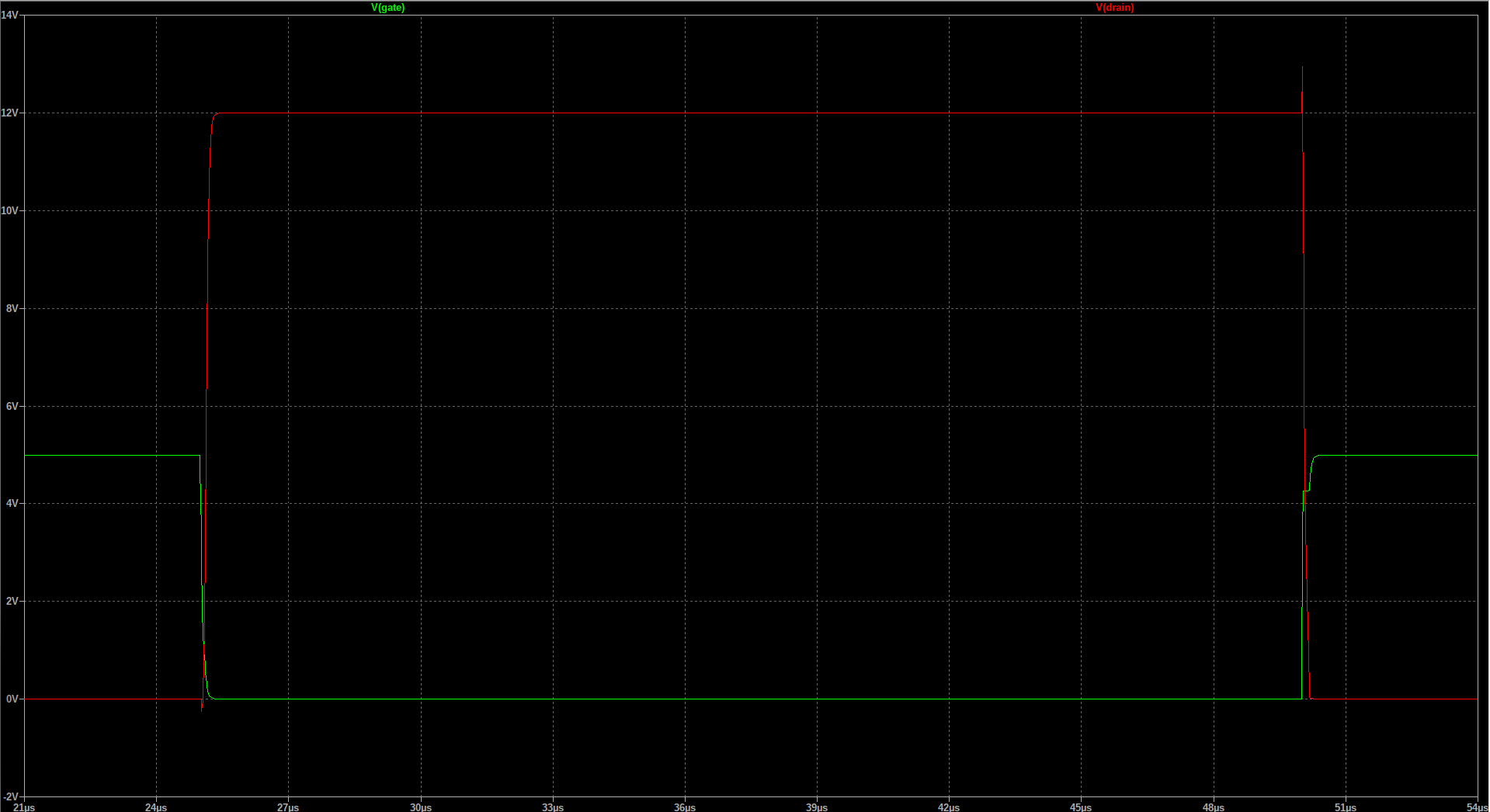
Figure 3 – LTspice simulation for Rg = 10 Ω.
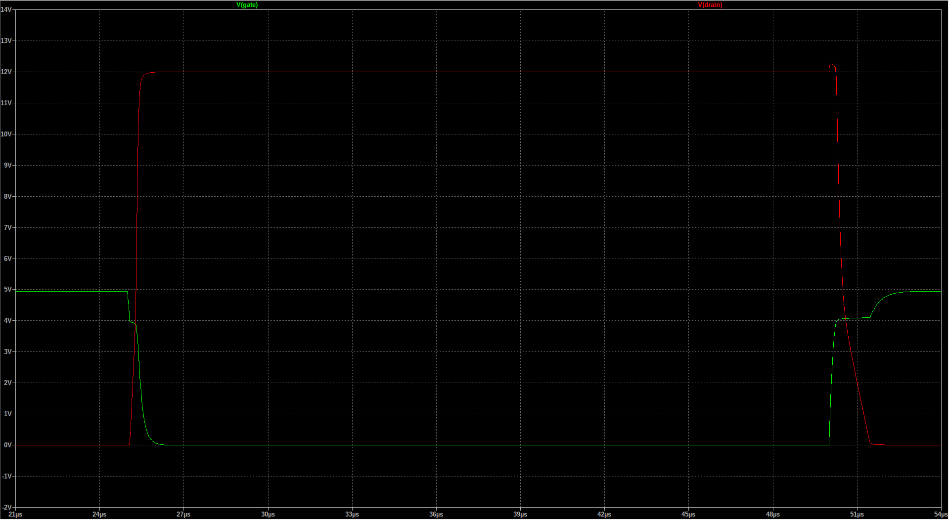
Figure 4 – LTspice simulation for Rg = 100 Ω.
Table 1 – LTspice transient simulation results showing the rise and fall times of the gate and drain voltages for Rg = 10 Ω and Rg = 100 Ω.
|
Parameter |
10R (ns) |
100R (ns) |
|
Gate Rise Time |
194 |
1680 |
|
Gate Fall Time |
116 |
641 |
|
Drain Rise Time |
120 |
260 |
|
Drain Fall Time |
109 |
915 |
5 Experimental Measurements
After completing the LTspice simulations, the same circuit was assembled and tested under laboratory conditions. Every effort was made to reproduce the simulation setup as closely as possible by using the same circuit topology, component values, supply voltage, and gate drive signal.
The gate and drain voltages were measured using a Siglent SDS2304X digital oscilloscope equipped with 10× passive probes. The MOSFET was driven by a Siglent SDG1062X function generator configured to generate a 0–5 V square wave at 20 kHz with a 50% duty cycle. Measurements were performed for both gate resistor values (10 Ω and 100 Ω) using the same methodology described in the previous section.
The oscilloscope’s built-in measurement functions were used to determine the rise time and fall time of both the gate and drain voltages, using the standard 10%–90% measurement criterion. The measured waveforms are presented in the following figures.
In all oscilloscope screenshots presented in this article, the yellow trace (Channel 1) corresponds to the gate voltage, whereas the purple trace (Channel 2) corresponds to the drain voltage.

Figure 5 – Oscilloscope measurement for Rg = 10 Ω
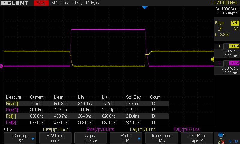
Figure 6 – Oscilloscope measurement for Rg = 100 Ω.
Table 2 – Oscilloscope measurement results showing the rise and fall times of the gate and drain voltages for Rg = 10 Ω and Rg = 100 Ω.
|
Parameter |
10R (ns) |
100R (ns) |
|
Gate Rise Time |
711 |
1660 |
|
Gate Fall Time |
362 |
836 |
|
Drain Rise Time |
183 |
301 |
|
Drain Fall Time |
370 |
877 |
6 Conclusion
As expected, the simulation and the experimental measurements show a very similar overall switching behavior. Although small differences can be observed in the measured rise and fall times, the general trends are well reproduced by the LTspice simulation. Increasing the gate resistor from 10 Ω to 100 Ω results in slower gate charging and discharging, which is reflected in both the simulated and measured waveforms.
The remaining discrepancies are expected and can be attributed to factors that are difficult to model perfectly, such as parasitic inductances and capacitances of the experimental setup, oscilloscope probes, PCB traces, wiring, component tolerances, and the limitations of the SPICE model itself.
Table 3 – Comparison of the measured switching parameters obtained from LTspice simulations and laboratory oscilloscope measurements.
| Parameter | LTspice 10R (ns) |
Osc 10R (ns) |
LTspice 100R (ns) |
Osc 100R (ns) |
| Gate Rise Time | 194 | 711 | 1680 | 1660 |
| Gate Fall Time | 116 | 362 | 641 | 836 |
| Drain Rise Time | 120 | 183 | 260 | 301 |
| Drain Fall Time | 109 | 370 | 915 | 877 |
Overall, the results demonstrate that LTspice provides an excellent prediction of the switching behavior for this relatively simple circuit and can therefore be considered a reliable tool during the early stages of electronic design.

Amar Degirmendžić
Senior Embedded Hardware Engineer
Amar Degirmendžić (E76DA) is an Senior Embedded Hardware Engineer and amateur radio operator interested in electronic system design, RF systems, and measurement techniques. His work ranges from schematic capture and PCB design to hands-on circuit assembly, testing, and practical laboratory measurements

S