
Parasitic capacitance and MOSFET
1 Introduction
In this blog, we consider the MOSFET transistor as a switch. We examine the influence of PCB trace length and geometry on the dynamic behavior of the transistor through measurements at three different frequencies and by comparing the input and output waveforms.
We consider the schematic shown in Figure 1, a simple diagram of the transistor used as a switch.
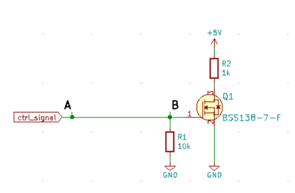
Figure 1 – A simple diagram of the transistor used as a switch
If we observe the control signal in an ideal world, the connection between the signal source and the MOSFET gate has no influence on the waveform. The voltage at the beginning, voltage UA, and the end of the trace UB is the same, and the transistor responds instantaneously to changes in the drive signal.
In a real PCB, this connection has distributed electrical parameters and can be approximated as a series R–L branch with capacitance to the reference plane:
trace resistance: Rtrace
trace inductance: Ltrace
capacitance to the GND plane: Ctrace
The MOSFET gate itself represents a capacitive load, most commonly described by the input capacitance:
Ciss = Cgs + Cgd
As a result, the drive source does not see only the transistor, but the entire network:
Rsource + Rg + Rtrace + Ltrace + (Ctrace || Ciss)
Such a structure behaves as a low-pass filter. Its approximate time constant can be estimated as:
τ ≈ (Rsource + Rg + Rtrace) · (Ctrace + Ciss)
The rise time of the gate signal is approximately:
tr ≈ 2.2 · τ
This means that increasing the trace length (and therefore Ctrace and Ltrace) directly increases the time required for the gate to reach the intended voltage.
In addition, changes in the drain voltage are coupled back to the gate through the capacitance Cgd. This phenomenon is known as the Miller effect and further slows the change of Vgs during transistor switching.
The practical consequence is straightforward:
-
-
- the longer the trace → the greater the total capacitance and inductance
- the higher the frequency → the stronger the influence of parasitic elements
- the gate signal becomes slower and smaller
- the transistor no longer turns on and off in the same way as in the ideal case
-
In the following sections, this effect is demonstrated experimentally by comparing short and long PCB traces at multiple drive frequencies.
1.1 Measurement Equipment and Methodology
The experiment was conducted using a Siglent SDG1062X signal generator and a Siglent SDS2304X digital oscilloscope. The drive signal was applied to the MOSFET gate through a 110 Ω series resistor, while the drain was loaded with a 1 kΩ resistor connected to a 5 V supply. The waveforms of Vgs and Vds were measured at several drive frequencies. On the same PCB, two variants of the connection between the drive signal and the gate were implemented: a short trace approximately 12 mm long, treated as a near-ideal reference, and a long trace 161 mm in length. The waveforms obtained on the short and long traces were directly compared to quantify the impact of PCB trace parasitic parameters on the dynamic behavior of the MOSFET.
Motivation for the Measurement
This investigation was motivated by a late-stage layout modification on an 8-layer PCB, where an additional long trace had to be introduced to drive a status LED without rerouting the rest of the design. Although the signal operated correctly due to its low switching requirements, it raised a practical question: how would a higher-frequency switching signal behave if routed through a similarly long trace? The present measurements were conducted to explore this scenario experimentally.
Since the same PCB contained both a short trace and this long trace (which changes layers several times), we used them for the measurements.
2 Measurement at 10 kHz
At 10 kHz, the difference between the short and long trace is minimal. The Vgs waveform on both traces follows the drive signal without significant distortion, with negligible differences in amplitude and rise time. In both cases, the MOSFET turns fully on, which is evident from the full switching of Vds between approximately 0 V and 5 V. In this regime, the parasitic parameters of the PCB trace do not have a dominant influence, and the connection between points A and B can be approximated as ideal.

Figure 2 – Waveforms: yellow (Vgs), magenta (Vds) on short trace at 10 kHz

Figure 3 – Waveforms: yellow (Vgs), magenta (Vds) on long trace at 10 kHz
3 Measurement at 100 kHz
At 100 kHz, a visible difference between the short and long trace appears. On the long trace, the Vgs amplitude is reduced and both rise and fall times increase, indicating a frequency-dependent loading of the gate due to the distributed RLC parameters of the trace. As a result, the MOSFET no longer transitions immediately into full conduction, and Vds exhibits a slower and incomplete transition. The short trace still shows behavior close to ideal, while the long trace clearly demonstrates the influence of parasitic capacitance and inductance.

Figure 4 – Waveforms: yellow (Vgs), magenta (Vds) on short trace at 100 kHz

Figure 5 – Waveforms: yellow (Vgs), magenta (Vds) on long trace at 100 kHz
4 Measurement at 1 MHz
At 1 MHz, the difference between the short and long trace becomes pronounced. On the long trace, Vgs is significantly attenuated and rounded, confirming that the gate drive is now bandwidth-limited by the Rg–trace–Ciss network. In this regime, the MOSFET does not reach full conduction, resulting in a smaller Vds swing and an apparently steeper transition due to reduced channel charge variation. The short trace maintains a higher drive level and more stable switching behavior, while the long trace clearly shows that the PCB connection must be modeled as a frequency-dependent element with distributed parameters.

Figure 6 – Waveforms: yellow (Vgs), magenta (Vds) on short trace at 1 MHz

Figure 7 – Waveforms: yellow (Vgs), magenta (Vds) on long trace at 1 MHz
5 Conclusion alternative
The measurements show a clear cause – and – effect relationship between the physical implementation of the connection and the dynamic behavior of the MOSFET. As the PCB trace length increases, the distributed parasitic parameters grow, leading to degradation of the gate drive – reduced Vgs amplitude and increased rise and fall times. As a direct consequence, at higher frequencies the MOSFET no longer operates in a fully switching regime but instead enters a partially enhanced region, which alters the dynamics of the Vds transition. The experiment confirms that the PCB trace between the drive source and the gate is not an ideal conductor, but a frequency-dependent element that must be considered in the design of fast switching circuits.

Amar Degirmendžić
Senior Embedded Hardware Engineer
Amar Degirmendžić (E76DA) is an Senior Embedded Hardware Engineer and amateur radio operator interested in electronic system design, RF systems, and measurement techniques. His work ranges from schematic capture and PCB design to hands-on circuit assembly, testing, and practical laboratory measurements

S