
LESSON 4 - Grounding in PCB design
While the basic concept of grounding is quite simple, implementation is very sophisticated.
For linear system, ground is the reference against which we base our signals. Unfortunately, it has also become the return path for power supply current in uni-polar supply systems. Inappropriate application of the ground system can destroy high accuracy linear system performance.
Some aspects of grounding that must be managed include the control of spurious ground and signal return voltages that can degrade performance. These voltages occurre due to external signal coupling, common currents or excessive IR drops in ground conductors. To control these parasitic voltages we implement proper conductor routing and sizing and differential signal handling.
This single issues of grounding can and will influence the entire layout of the PCB.
Modern signal processing system require mixed-signal devices such as analog-digital converters (ADC), digital-to-analog converters (DAC) and fast digital singal processors(DSPs. To maintain low noise in digital environments is dependent exactly on including proper signal routing, decoupling and grounding
All sampling ADCs ( ADCs with internal sample-and-hold circuit) suitable for signal processing applications operate with relatively high speed clocks with fast rise and fall times ( a few nanoseconds) and must be treated as high speed devices, even though the output rates may appear low.
Mixed-signal ICs have relatively low digital currents, while others posses high digital currents. In many cases both analog and digital ports must be treated differently with respect to optimal grounding.
Separated Analog and Digital Grounds
Digital circuity is quite noisy. Saturating logic such as TTL and CMOS, draw large, fast current spikes from supply during switching. However, logic stages with hundred of milivolts(or more) of noise immunity, usually have little need for high level of supply decoupling.
Analog circuity is quite vulnerable to noise on both power supply rails and grounds. Which means it is very sensible to separate analog and digital circuity.
To prevent digital noise from corrupting analog performance involves separating both grounds return and power rails, which in inconvenient is a MIXED SYSTEM.
If a mixed signal system is to provide full performance capability it is essential to have separate analog and digital grounds.
For example, some analog circuity will operate(function) from a single +5V supply but it does not mean that is should operate from the same noisy +5V supply as the Microprocessor or dynamic RAM.
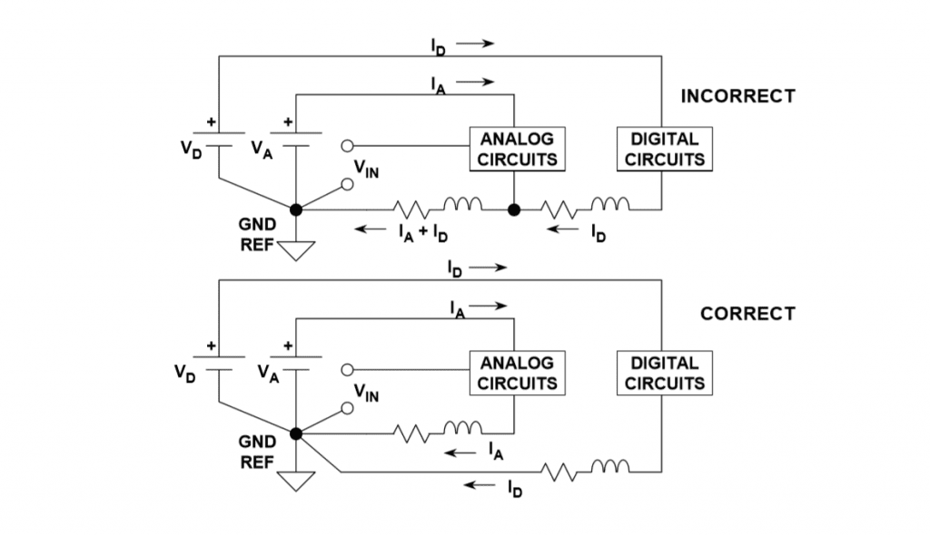
With all this emphasis on separation of analog and digital grounds, in a system they have to be joined together at some point. One of the ways to achieve that is to use STAR GROUND, star point or simply analog and digital ground having dinner point. This point is chosen so that it does not introduce digital currents into the ground of the analog part of the system. It is often continent to make the connection at the power supplies.
Note, some ADCs and DACs have separate analog ground(AGND) and digital ground (DGND) pins. Users are often advised to connect these pins together at the package.
The labels ‘’analog ground’’ and ‘’digital ground’’on these pins refer to the internal parts of the converter to which the pins are connected, and not to the system grounds to which they must go.
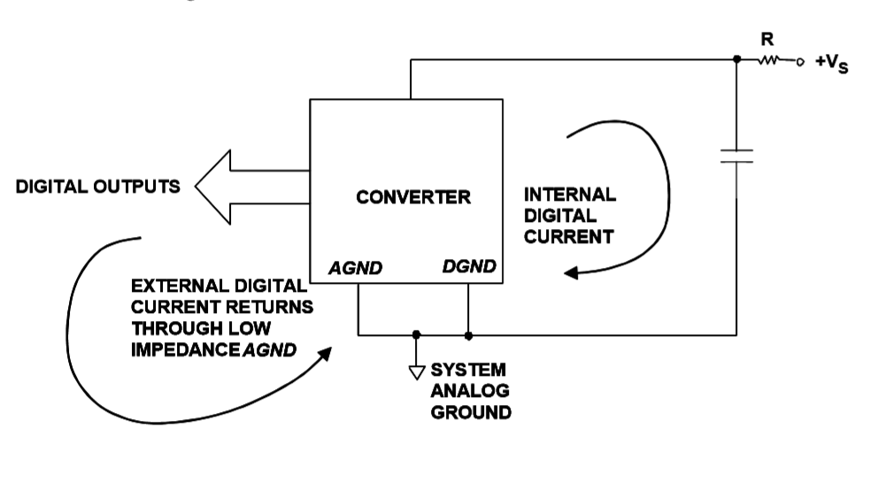
For example, with an ADC, these two pins should be joined together and to the analog ground of the system. It is not possible to join these pins inside the IC package, because the analog part of the converter can not tolerate the voltage drop resulting from the digital current flowing in the bond wire to the chip, But they can be tied – externally.
Ground planes
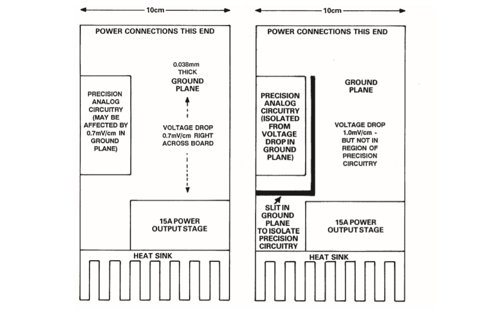
Related to the start ground system discussed earlier is the use of a ground plane. The theory behind this is that the large amount of metal will have as low resistance as possible. It will, because of the large flattened conductor pattern, also have as low an inductance as possible. It offers the best possible conduction, in terms of minimizing spurious ground difference voltage across the conducting plane.
But even a continuous sheet of copper foil has residential resistance and inductance, and in some circumstances, can be enough to prevent proper ground function.
PCB designers should be wary of injecting very high currents in a ground plane as they can produce voltage drops that interfere with sensitive circuity.
The ground plane acts as a low impedance return path for decoupling high frequency currents caused by fast digital currents but also minimizes EMI/RFI emissions. Because of this shielding action of the ground plane, the circuit’s susceptibility to external EMI/RFI is also reduced.
Power supply pins should be decoupled directly to the ground planes using low inductance ceramic surface mount capacitors. If THT ceramic capacitors are used, their leads should be less that 1mm. The ceramic capacitors should be placed as close as possible to the IC power pins.

Benjamin Hodžić
Intern
S