
HOW TO REVERSE ENGINEER GERBER FILES
Reverse engineering Gerber files into PCB layout file
Gerbers?
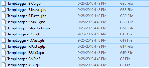
Gerber files are a file format used in the PCB industry for manufacturing of printed circuit boards. It is a standardized file format, no matter which CAD system is used the files will have the same extensions;
- Top Silkscreen .gto
- Top Copper .gtl
- Top Solder mask .gts
- Inner layer 2 .g2
- Inner layer 3 .g3
- Bottom Silkscreen .gbo
- Bottom Copper .gbl
- Bottom Solder mask .gbs
- Edge Cuts .gm1
- Drill files .txt
We have already elaborated how to generate Gerber files and how to send them to a manufacturer, you can find a video with full instructions in the guides section.
In this topic we will concentrate on a feature that is present in KiCAD and teach you how to make changes to a board if gerber files are all you have got.
Reverse Engineering?
Here is the situation; you have been given Gerber files and need to fix a problem on the board. Now comes the question, how am I to open the board in my PCB layout editor and make adjustments if I just have gerber files?
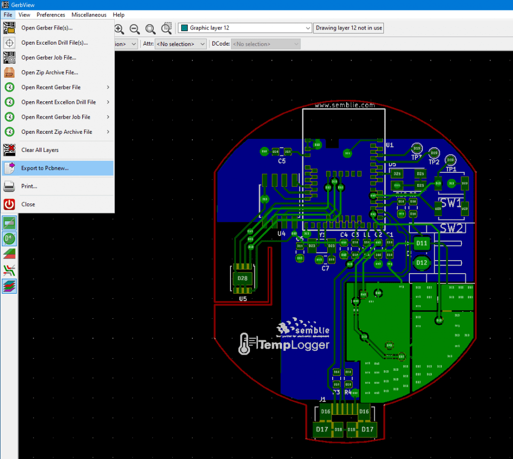
Lets first load our Gerber files into KiCAD with the Gerber viewer module
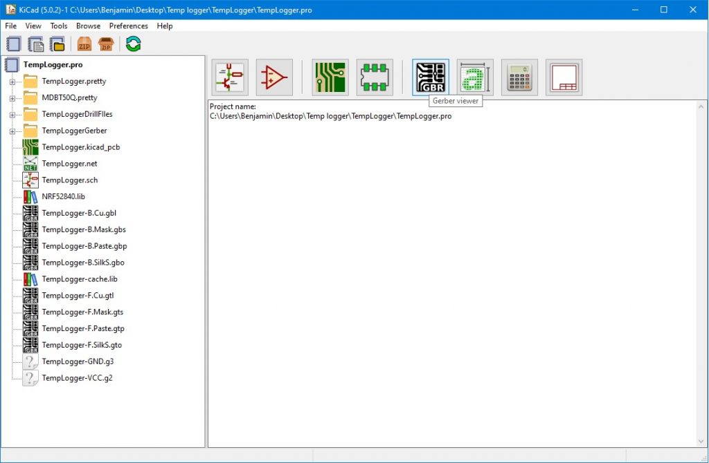
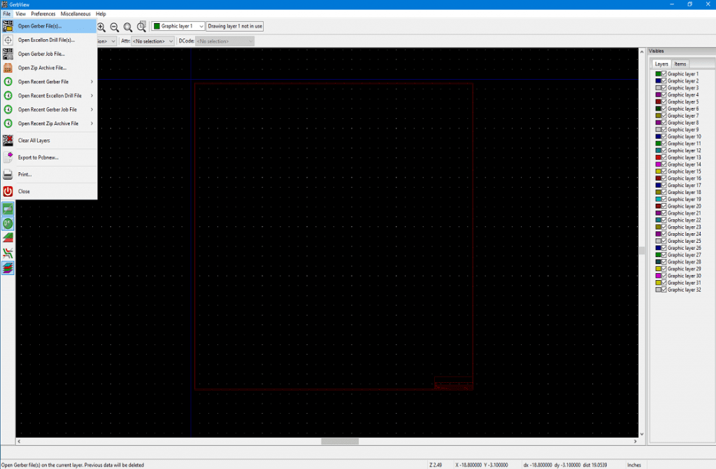
After we have imported all required files, our board gets loaded in. Now we can see all the layers and components that were used.
The Gerber viewer module allows you just to observe the board. If we want to make adjustments we need to open the board in the PCBnew module (layout editor). To do that, go to Files and select Export to Pcbnew. A new window will open and you will have to select where do you want to save your new layout editor file.
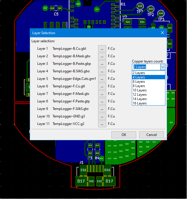
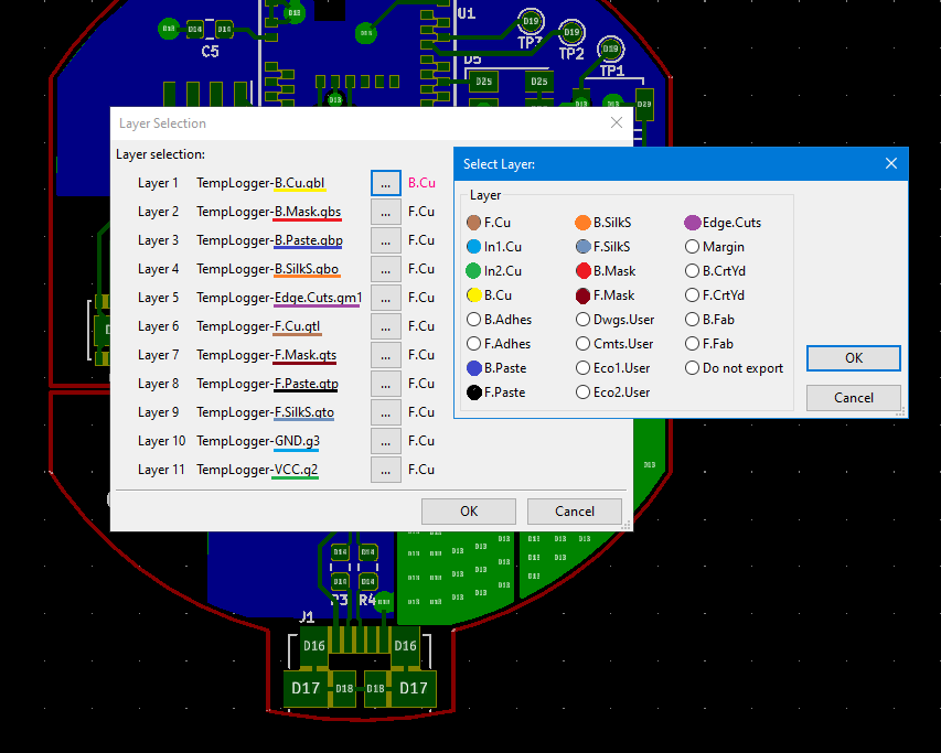
Select how many layers does the board consists of and you will have to reassign these layers. Don’t get afraid of this process, to see how many layers the board is made of just look at your Gerber files. If there are no .g2 .g3 files it is a 2 layer board and if they are present it is a 4+ layers board. For layer re assignation, the layer name should be in the name of the Gerber file just select it again
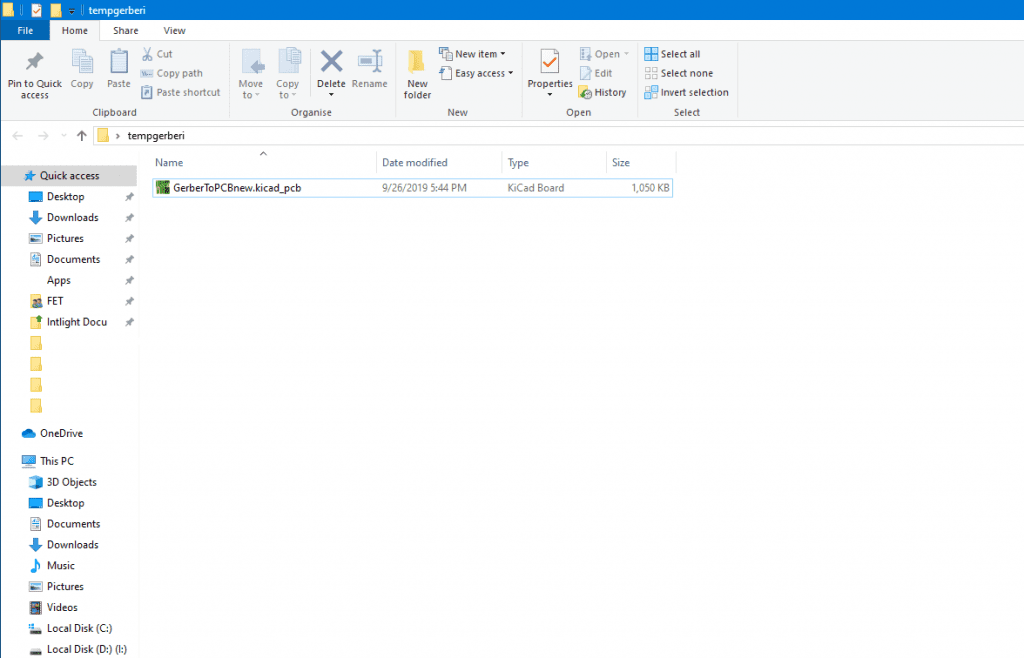
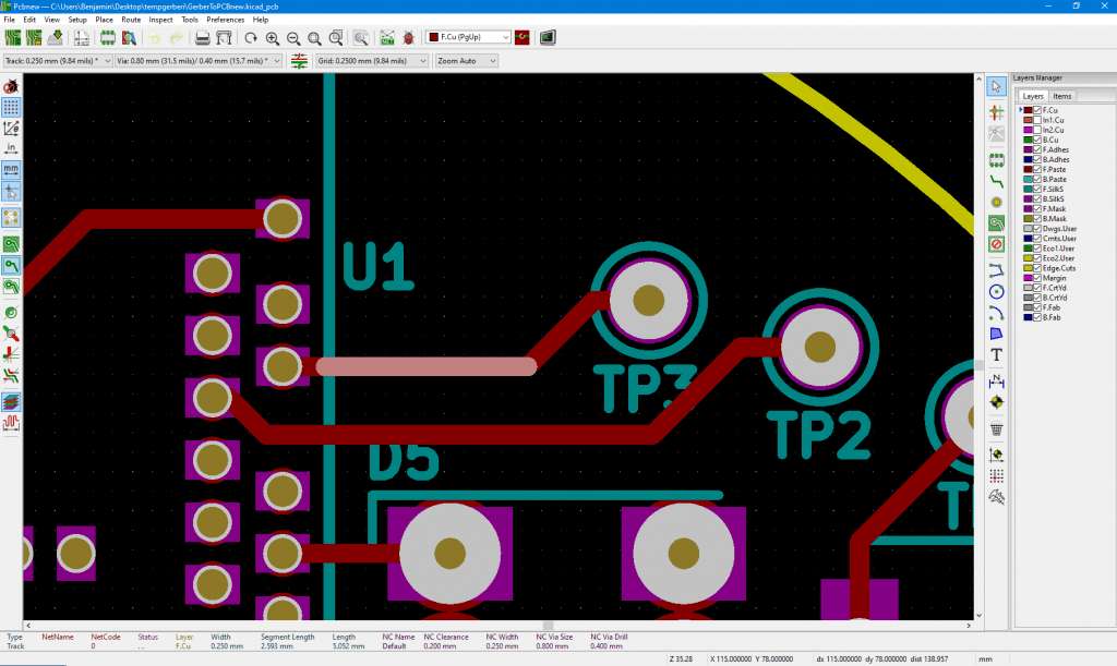
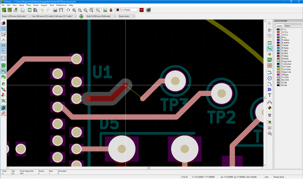
After clicking OK and generating your new PCBnew file you can open it now and make your adjustments.
Don’t forget to plot the Gerber and Drill files again before sending them for manufacturing.
Good luck !

Benjamin Hodžić
Intern
An electrical engineering student from Bosnia. He’s doing the apprenticeship at Semblie d.o.o. Tuzla.
S