Experience with the design of a high-speed interface
As a beginner in the design of electronic devices, one usually works on designs that are less complex. These are usually just simple, 1 or 2-layer boards. Not to say that these can’t be complex and used in real devices, but things do get a lot more complicated when dealing with multilayered boards.
As the years went by I got to experiment with different fields of electronics, but one of those that stuck with me the most to this day is PCB engineering. That’s why I decided to give a brief summary of the methods of PCB design and assembly I’ve worked with through these years.
Designing for FPGA can be a challenge
The first project that put some sweat under that thinking cap of mine was the one in which we had to deal with FPGA. Since the device requires FPGA, it also requires high-speed processing. This tells us that the assembly has at least one high-speed interface for processing/exchanging data.
To be more specific, the device that I designed uses RGMII high-speed interface for the communication between FPGA and Ethernet PHY IC. The first thing that popped into my mind was: “Will I be able to do this…?”. This is something I often ask myself, but in the end, with enough dedication and work, everything gets done so will this. Education and professional development are something every engineer encounters on a daily basis, especially in R&D work. A colleague of mine that works with me on many of these projects always keeps saying his words of wisdom: “Take it easy… It’ll get done…”. It somehow brings me comfort.
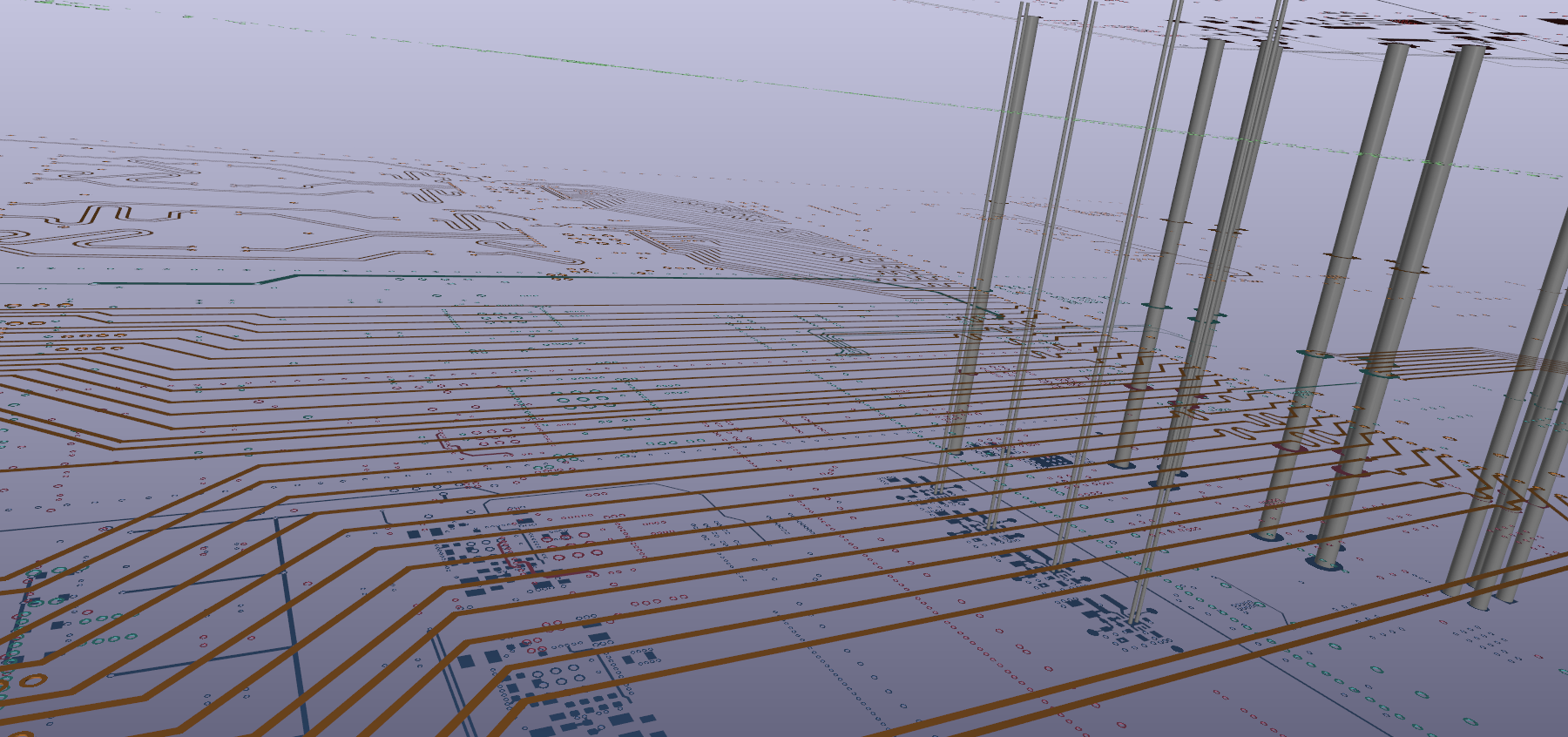
If you ever try designing an RGMII interface on a 2-layer PCB with the standard stackup even if you follow parameters of just the impedance and length matching, you’ll realize what difference in physical limits between the 2-layer and multilayered PCBs. Adding the standards to all of this is just the cherry on top.
What else should be taken into consideration?
The designed RGMII interface has a max data rate of 250Mbit/s and operates on a frequency of 250MHz, edge rise/fall time is 750ps. All traces in the RX bus have to have a single-ended impedance of 50ohm and they have to be the same length. The same stands for the TX bus. Vias on these traces also introduce additional impedance, capacity and length. Therefore, special considerations should be taken into account when designing the vias as well. If one trace in the RX trace band has one passing from one layer to another, all other ones must be the same, and the same goes for the TX traces. It is suggested for this type of interface to be routed in a single layer if possible. Lengths of RX and TX buses have to be the same, but just to the same type. RX and TX traces don’t have to be of the same length which makes the job a bit easier when dealing with tight space on the PCB.

Well, one might wonder now how sensitive the RGMII interface is to the different impedance and trace lengths. Luckily, not much, at least in my experience. During the development process, we made a few mistakes with the interface itself. The mistakes like different lengths of the traces, different impedance, crosstalk on the boundary, and routing of the same buses on different layers.
Impedance varied from 47 to 51 ohm on the same RGMII interface. Differences in the trace lengths went even up to 5mm, and some traces in the same RX bus of one RGMII interface were routed in the top layer and some on the inner layer of the PCB. Even with these shortcomings, the device worked with satisfactory performance results. These shortcomings were fixed in the next iteration of the design.
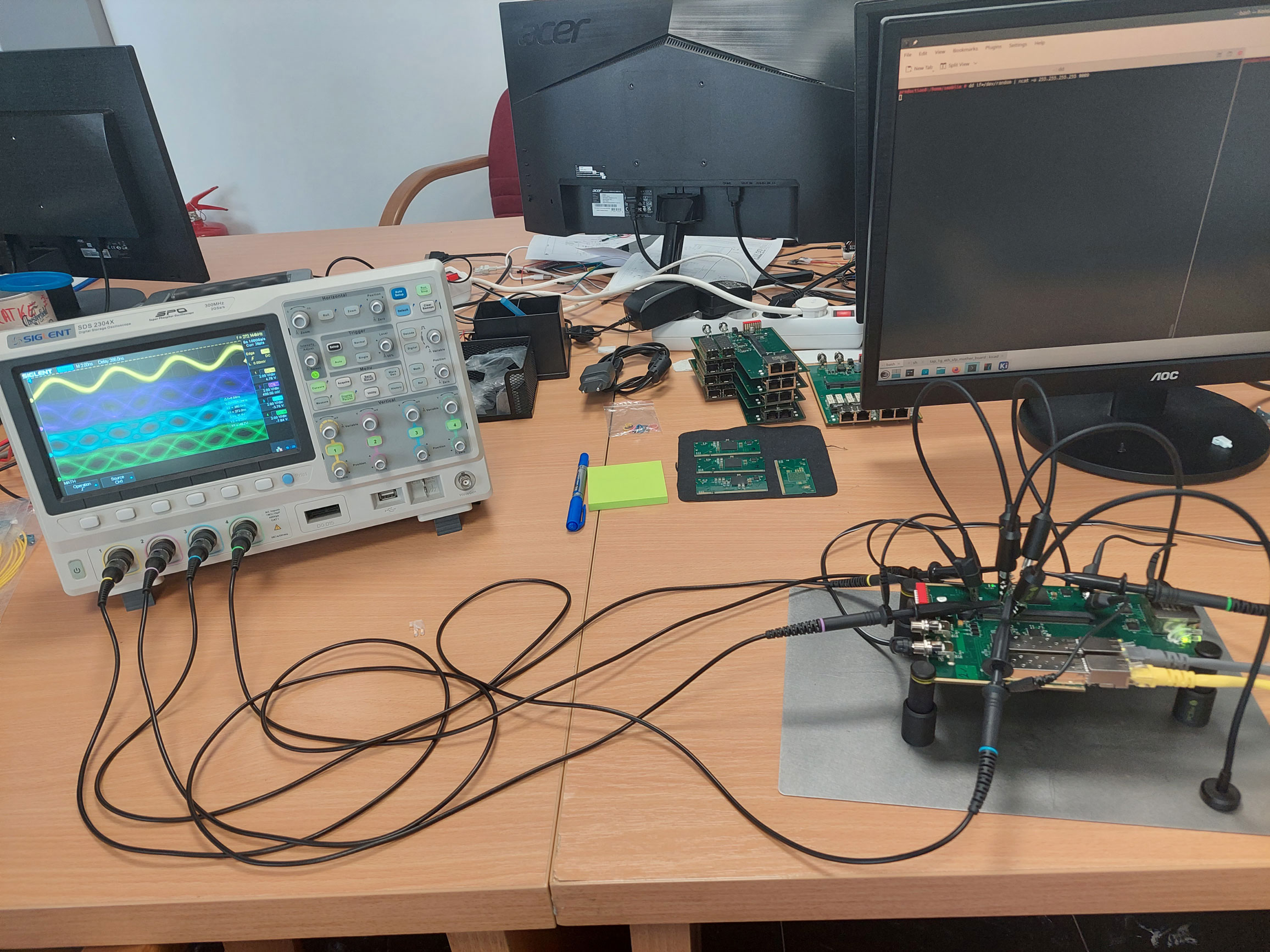
The best way to get feedback about the quality of the interface design is to make some measurements. To get these measurements with good accuracy we need good enough equipment and predefined measuring points. In the case of the high-speed interface are not viable in form of a simple test point. We discovered this the hard way when we found that we didn’t have adequate test points on the device. This of course made measurements quite difficult.
The method that can give you some feedback is generating an eye diagram using the oscilloscope. Eye diagrams can give us information about the jitter, crosstalk, signal amplitude and others.

Learning through challenges
This project was a great opportunity to introduce myself to impedance matching, length matching, crosstalk and all other parameters that are necessary for a good design of one of these interfaces. Component manufacturers give pretty good design guidelines for high-speed interfaces that are being used. If we follow it we should be able to get the desired functionality.
The evidence is the fact that the device we designed works as intended, even passing all of the functionality tests. It even passed the compliance tests like CE without any issues.
About the author

Tarik Nurkanović
Co-Founder, CEO and Chief Hardware Engineer
Tarik is our CEO and co- founder. His favourite role tho, the one that he always runs back to, is chief hardware engineer. His specialties are PCB design, both analogue and digital electronics, but working with hardware directly brings him immense joy that is beyond all else.

S