PCB Design and Development Process
Today, the development process is unimaginable without the appropriate software tools. A few years ago, these tools were much more difficult to acquire.
We will mainly focus on design considerations in the development of electronic devices, more precisely in the development of PCBs. When solving any problems, knowledge comes first. Software tools allow us to put an idea into action, that is, to generate the necessary files on the basis of which the PCBs will be produced. The difficulty of this process, of course, depends on the complexity of the device.
There are many different software tools for the design of electronics on the market today. Some of them are free, the most popular one being KiCAD, which is considered a hobby tool. Some of the most popular professional software tools of this kind are Altium designer, Eagle and Cadence Allegro.
The advantages of these professional tools are that they have a lot of very useful integrated features that make the work much easier. The features like simulators and routing tools are just among many others.
Basically, the wiring diagram of the electronic device contains just the information about the connections between the components of the system only, and it does not give us any information about their relation to the PCB.
The functionality of the device itself is in the first place, of course, but immediately after that comes the reduction of the noise levels to such an extent that it does not interfere with the operation of the device. In order to enter the market, every device must comply with certain standards. The condition for this is to pass the compliance and safety tests for a given standard. For example, this is used to get qualified e.g. CE or FCC mark.
But, what do the standards have to do with the PCB itself? In a vast majority of cases, poor routing and poor selection of PCB parameters will cause poor EMI and EMC testing results. These are unavoidable for any electronic device.
Based on the analysis of the electrical diagram and the analysis of other technical requirements for the device, the PCB designer selects the already existing PCB stack from the manufacturer or adjusts the PCB stack in the case of a premium PCB service. These cost more, but the manufacturer makes the PCB stack as desired, which is necessary for high-performance devices.
There are several steps required for a PCB to be ready for the manufacturing of the functional prototype. This prototype still requires some corrections in 99% of cases, but at the minimum, the required steps are as follows:
- Electrical schematic design
- PCB stack-up setup
- PCB design rule setup
- PCB routing
- Design rules check
- Fabrication outputs Generating Gerber, Drill files, Generating bill of materials – BOM
The next step is to prepare and send the files for manufacturing. PCB manufacturing can be in-house or outsourced to PCB manufacturers.
In the beginning, we’ve been doing in-house PCB manufacturing using the tools that were available at the time. This was not enough to get the quality acceptable for a prototype. It was just good enough for some simple assemblies. Today, PCB manufacturing is very affordable, so much so that for a few bucks you get really high-quality PCBs that are way beyond anything that could be done with a few simple tools in-house.
After we get the prototype, testing can begin. As for the in-house assembly process, quality can be comparable to the ones done by the manufacturer. Considering that most PCBs today are done with SMT technology, a good solder paste, stencil printer and a steady hand can do just about anything when it comes to the production of a prototype.
For batches of ten or more assemblies of relatively more complex devices with a few hundred components, a pick and place machine can be of great help (if you know what you’re doing).
Testing an electronic device can involve several different tests, some of which are:
- Functionality Testing
- Electrical testing
- EMI testing
- Testing in operating, storage and transport conditions
As we already listed some of the steps in the PCB development process, we will now go through some of the more important ones in more detail.
Electrical schematic design
Electrical schematic design should, alongside the functionality of the device, follow certain rules in regards to hierarchy and order. It needs to be readable with as many details as possible to ensure that we have all the necessary information that may be needed in the steps that follow the electrical schematic. Some of the examples are:
- I2C device address (suitable for embedded developers)
- Routing information for the USB interface
- Link to a reference design of a specific IC
- High voltage circuit (specially marked)
- Description of the functionality of a specific part of the circuit
It’s best to have the electrical schematic organized in blocks. Altium designer offers one of the better solutions for this. The circuit diagram is the input for PCB design
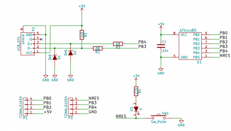
Example of electrical schematic
PCB stack-up setup
There are several PCB stacks available on the market. They differ in the number of layers (1, 2, 4, 8 and more), the thickness of the conductive layers (Cu), and the thicknesses and materials of insulator layers (PrePreg and Core).
In terms of price-performance ratio, PCBs with fewer layers (1,2 or 4) are cheaper but may perform worse, while PCBs with more layers cost more but may provide better performance. The term PCB performance is relative as it depends on the complexity of the device itself. Some devices can be perfectly implemented on boards with a small number of layers.
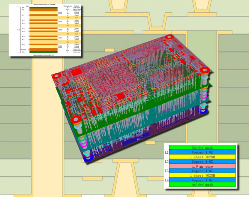
Example of PCB stack-up setup
The most common insulator material is FR4. Its performance can meet the needs of the widest range of electronic devices. By choosing the right PCB stack and material, we have the opportunity to reduce the risk of EMI, reduce the level of noise in the circuit, and achieve a better signal of integrity.
By choosing the right PCB stack and material, we can reduce the risk of EMI, and the level of noise in the circuit, and achieve better signal integrity.
PCB design rule setup
Every manufacturing process has its limits, and so does PCB manufacturing. The manufacturer sets a minimum technical specification for his manufacturing process, which has to be followed during the design. This is done to ensure that the PCB will be produced without errors. Some of the more common specifications are:
- Minimum drilling hole
- Minimum line spacing
- Minimum silkscreen text size
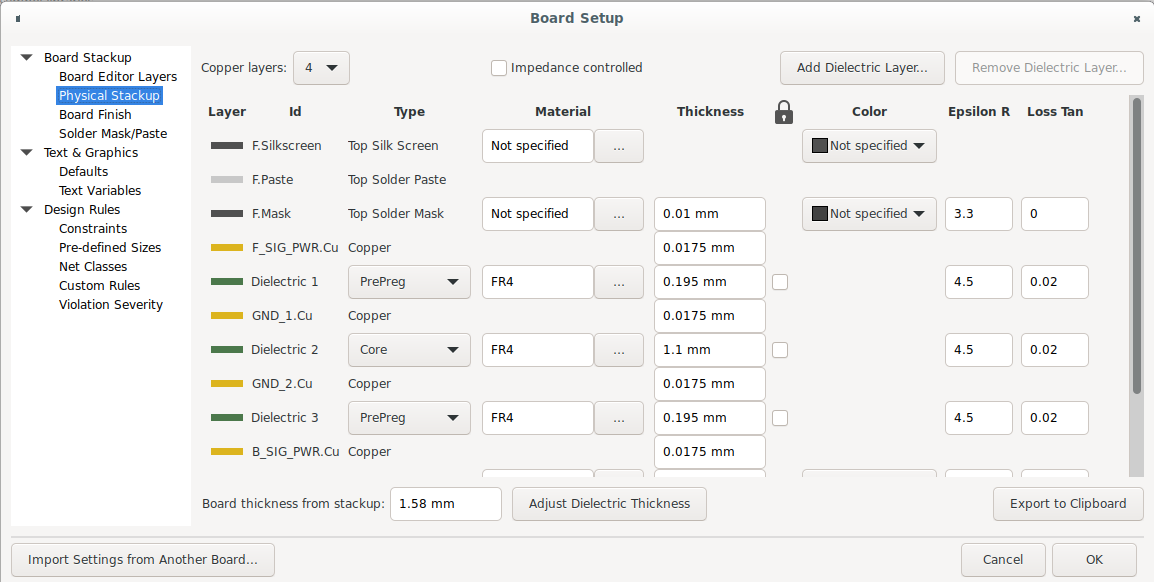
Example of PCB Design rule setup
PCB routing
This is one of the most important steps. Special care must be taken of:
- PCB layout (must suit all functional, electrical and temperature properties)
- Signal integrity (there are many parameters that have to be considered)
- Order and hierarchy are very important
- Noise reduction
- Electrical parameters of traces
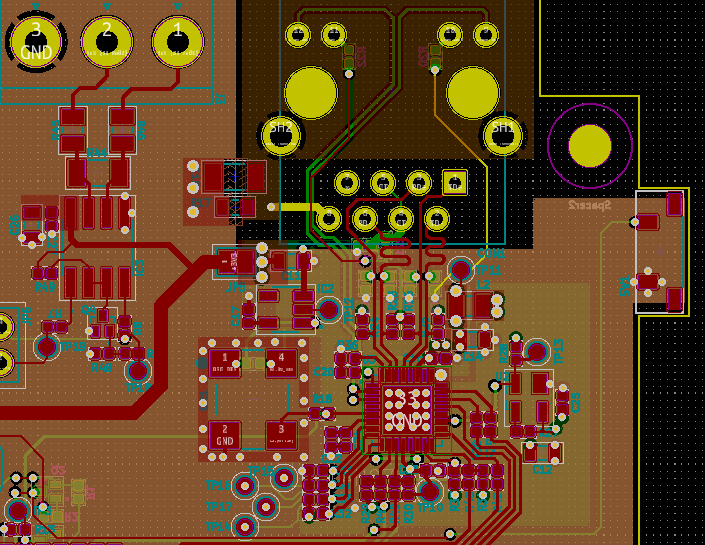
Example of PCB routing
Design rules check
The software tool is used to check if everything is in accordance with the design rule setup. Some beginner designers often skip this step, but it is highly useful and important for the reduction of mistakes in the PCB design process itself.
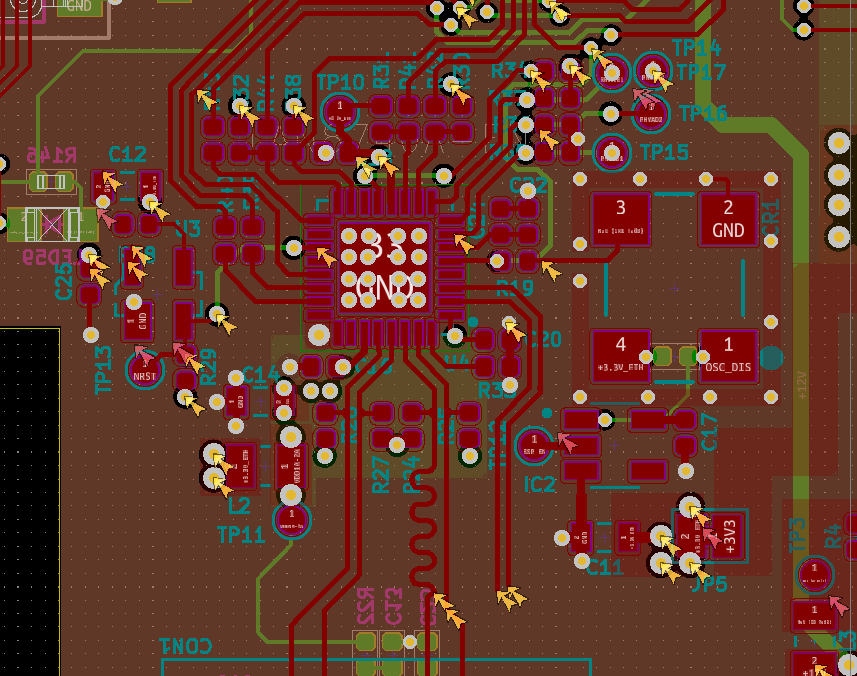
Example of design rule check output
Fabrication outputs
After all previous steps are finished, we can proceed to the generation of manufacturing files.
Files that need to be generated are:
- Gerber files
- Drill files
- Bill of Materials (BoM)
- PCB stack
- Pick and place files
There are several formats for generating these files. Different software tools provide different properties for Gerber file generation. The file format is selected per the requirements provided by the PCB manufacturer.
In-house PCB manufacturing vs regular PCB manufacturing
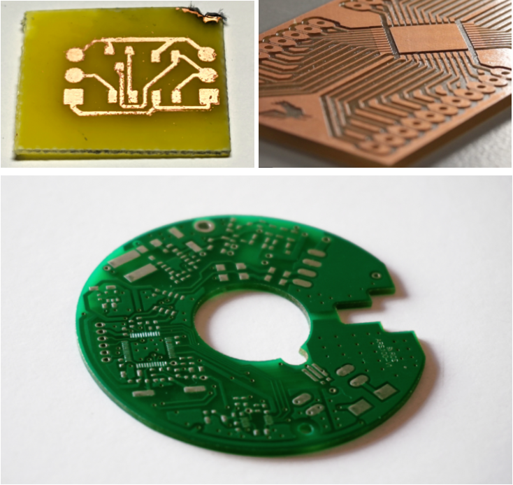
In-house PCB manufacturing can be done in one of the following ways:
PCB milling process
- CNC machine removes the unwanted surface-layer copper
- CNC machine drills the holes and cuts the edge
- Does not require masking
- Does not require additional chemical processing
PCB etching process
- The chemical process is used to remove the unwanted surface-layer copper
- Requires masking as follows:
- Photo film procedure
- Film transfer
- Printing the mask directly
- Hole drilling afterwards
Both of these processes limit PCB manufacturing to a max 2 layer PCBs, which is enough for a quick test of simple devices or parts of complex devices.
Furthermore, these processes cannot provide the results that we get with regular PCB manufacturing. Even at the start, we’re limited to:
- Number of PCB layers to 2 max
- PCB stack and PCB materials (available on the market)
- Precision (e.g. BGA components are all but impossible)
- Quality
About the author
Tarik Nurkanović
Co-Founder, CEO and Chief Hardware Engineer
Tarik is our CEO and co- founder. His favourite role tho, the one that he always runs back to, is chief hardware engineer. His specialties are PCB design, both analogue and digital electronics, but working with hardware directly brings him immense joy that is beyond all else.

S
