In-house PCB manufacturing
Even as a kid, I’ve shown quite a bit of interest in the matters of technology, and above all, electronics. I’ve been blessed with the good fortune of having an engineer for a parent. My dad was an engineer experienced in the fields of electronic and control engineering, so I’ve had the opportunity to learn everything I was curious about… and, of course, I squeezed every opportunity I had.
As the years went by I got to experiment with different fields of electronics, but one of those that stuck with me the most to this day is PCB engineering. That’s why I decided to give a brief summary of the methods of PCB design and assembly I’ve worked with through these years.
Carbon paper
I did my first PCB when I was 11. Back then I was not even aware of the software for PCB design, and at the same time, these were not really that accessible. My first PCB was done following these steps:
- The traces and components are drawn on the basis of the electrical schematic
- Alcohol or some other substance with similar properties is used to clean the surface of the phenolic/pertinax board
- The traces on the paper with the sheet of carbon paper below are followed to transfer them onto the copper of the board
- Transferred traces on the copper are followed by a permanent marker
- The board is submerged into the solution of hydrochloric acid, hydrogen peroxide and water. This will etch the copper where nothing is drawn
- After the etching process is done, holes for the components can be drilled in
- Components can be soldered now using the soldering iron
In the beginning, I used this method to learn the basic principles of PCB manufacturing and assembly. With this method, I was able to make single-layer boards. Double-layer boards can be done but it can be difficult. The method is suitable for THT components. It can be used maybe for some hobby projects as it is quite imprecise and difficult to implement well, but it’s rarely used even for that.
Toner transfer
This method requires a PC and a laser printer. PCB traces can be drawn in any graphic software tool, but CAD software for PCB design would be the best of course. There is transfer paper for this purpose on the market, but a humble flyer paper does just fine …in my own experience at least.
A laser printer is used to print the traces onto the transfer paper. The transfer of the toner to the copper can be done by using a clothes iron or a laminator machine.
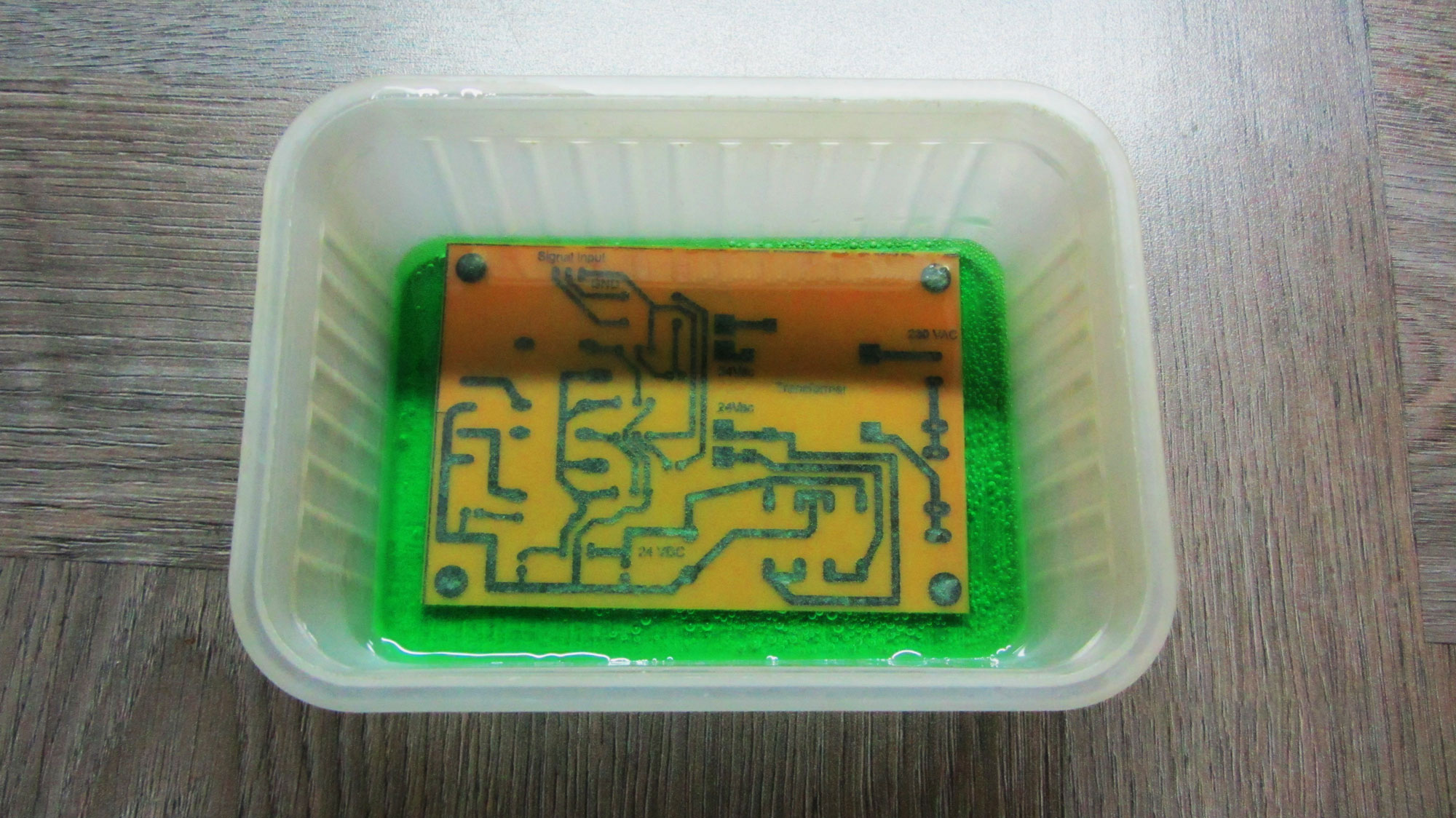
The rest is the same as in the previously described process (etching, drilling, soldering).
This is a more precise method for making PCBs as it enables creating the PCB for even some SMD components (e.g. 0805 and larger, SOIC and others). It can be used for simpler prototypes, but not for commercial applications.
Going from the first method to this… oh what change it was. This is something that I’ve been practising as a middle school student, and even later as a student of electrical engineering. After this, I’m starting on freelancing projects with my colleague and co-founder Amar.
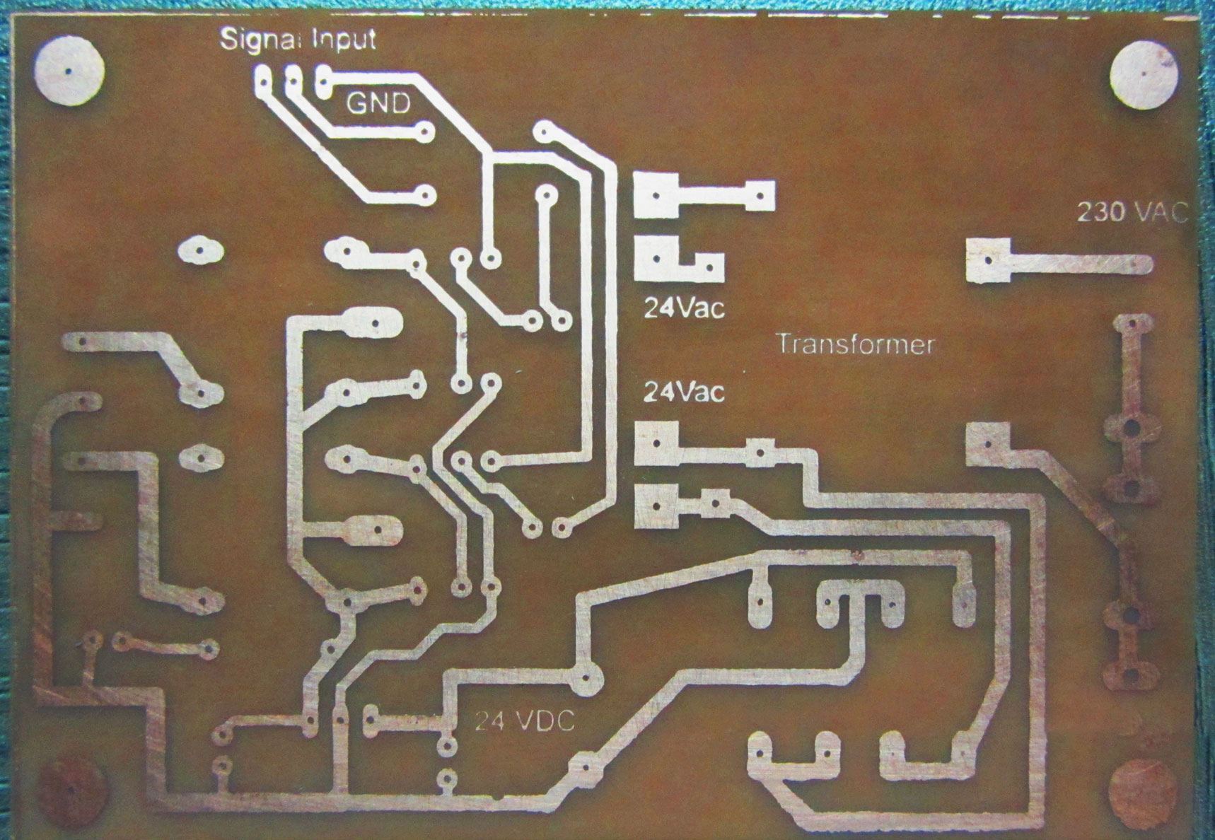
Both of the previously described methods can be problematic in regards to the quality of the traces. The transfer of some of the traces can fail, which results in a break. Double-layer PCBs are all but impossible to make using this method.
Photoresist
This was one of the methods that were also practised at the time.
Using this method we could do double-layer PCBs. In the beginning, we used this method for our freelance projects. Compared to the other two, this method also differs in the transfer of traces onto the copper surface.
This method requires the use of photoresist spray (e.g. Positiv 20 or similar), or, which is a much better option, the use of pre-sensitized photoresist coated FR4 PCB laminates. We, of course, used the pre-sensitized photoresist coated FR4 PCB laminates.
Steps for transferring the traces onto the copper surface:
- Traces that need to be transferred are printed onto the transparent film
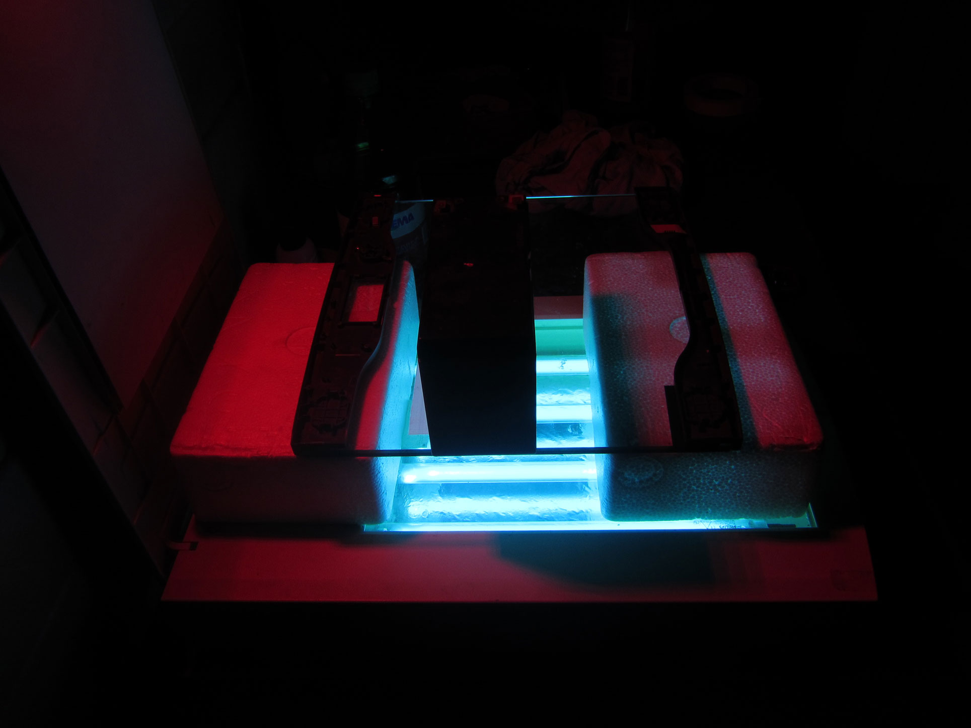
- The process needs to be done in a darkroom as boards should not be exposed to the sunlight
- The side that has the print is placed facing the copper surface and the film is pressed by the transparent glass to ensure the best coverage of the copper by the traces
- The boards are now exposed to UV light for 3 to 5 minutes (the period is determined experimentally and depends on the light used)
- Before etching, the boards are submerged in a solution of caustic soda
- The surface that was exposed to the UV light will be etched as in the previous methods described
- The rest of the process is the same as with the previously described methods
This method gives good results in regards to the precision, and the trace width can go down to 0.2mm. It can also be used to get the footprints for SMD components. A solder mask can be applied onto a PCB made in this way using a similar method. Photo-sensitive solder mask is applied to the PCB. A transparent film is placed onto it, and then the stencil. Everything is pressed by the transparent glass and exposed to UV light for some time. The solder mask exposed to light is set. The surfaces that were not exposed to UV light can be removed with acetone scrub.
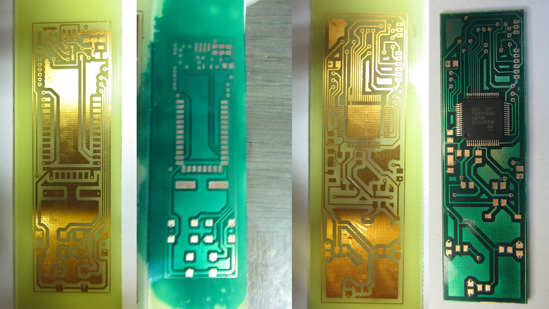
With all that being said, these processes are great only for the hobbyist, beginner and maybe for educational purposes and are incomparable in quality to the ones manufactured at the factory.
About the author
Tarik Nurkanović
Co-Founder, CEO and Chief Hardware Engineer
Tarik is our CEO and co- founder. His favourite role tho, the one that he always runs back to, is chief hardware engineer. His specialties are PCB design, both analogue and digital electronics, but working with hardware directly brings him immense joy that is beyond all else.

S
